The Art And Science Of Epitaxial Wafer Design: Unveiling The Key Elements For Semiconductor Success5/25/2023 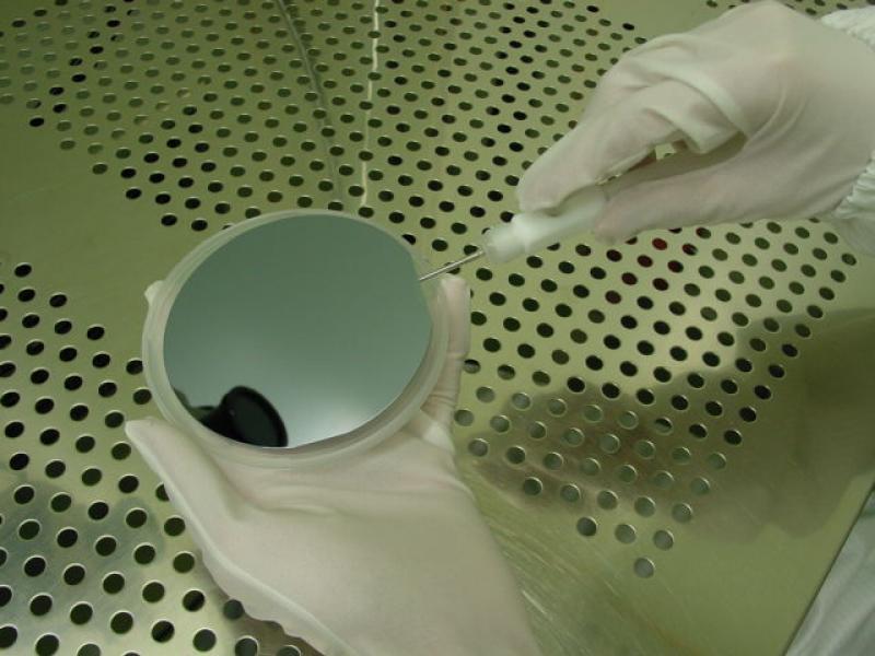 Epitaxial Wafer Epitaxial wafer design plays a crucial role in the world of semiconductor manufacturing, where precision and innovation are paramount. By understanding the art and science behind epitaxial wafer design, engineers and researchers can unlock new possibilities for advanced electronic devices.
Epitaxial Wafer design involves the precise deposition of semiconductor materials onto a substrate, allowing for the growth of high-quality crystalline layers. The epitaxial layer's composition, thickness, and doping profiles are carefully engineered to enhance the performance and functionality of electronic devices. By tailoring these parameters, designers can optimize characteristics such as carrier mobility, power efficiency, and device reliability. Material selection is a critical aspect of Epitaxial Wafer. Semiconductor materials, such as silicon, gallium arsenide, or indium phosphide, must be carefully chosen based on the desired device characteristics and operating conditions. Each material offers unique properties that can influence the device's performance. By leveraging advanced material characterization techniques and thorough analysis, engineers can select the optimal combination of materials for specific applications, ensuring the success. The art of Epitaxial Wafer design lies in achieving optimal device performance and efficiency. Designers must consider factors such as crystal orientation, layer thickness, and doping concentration to control carrier transport and minimize defects. By carefully engineering the epitaxial layers, it is possible to enhance charge carrier mobility, reduce leakage currents, and improve overall device efficiency. Moreover, optimizing the epitaxial wafer design for specific applications enables the creation of high-performance devices with superior functionality. To stay at the forefront of the semiconductor industry, Epitaxial Wafer design must integrate advanced manufacturing techniques. Techniques such as molecular beam epitaxy (MBE) and metal-organic chemical vapor deposition (MOCVD) enable precise control over layer growth, doping profiles, and interface quality. Process optimization and automation technologies enhance production efficiency, reducing costs and time-to-market. By leveraging these advanced techniques, manufacturers can meet the growing demand for cutting-edge in various industries. Epitaxial Wafer design represents the intersection of art and science in the semiconductor industry. By understanding the intricate details of material selection, optimizing performance and efficiency, and incorporating advanced manufacturing techniques, engineers and researchers can push the boundaries of electronic device capabilities. The artistry lies in the careful crafting of epitaxial layers, while the science ensures the precision and reliability of the resulting devices. With continued advancements in design, we can anticipate a future where electronic devices are more powerful, efficient, and versatile than ever before. The field of Epitaxial Wafer design is witnessing a rapid expansion in its applications and is poised to revolutionize multiple industries. From telecommunications and optoelectronics to renewable energy and healthcare, enabling breakthroughs in a wide range of fields. As research and development continue to push the boundaries of material science and device design, we can expect even more innovative applications in the future. With the integration of emerging technologies like artificial intelligence and quantum computing, epitaxial wafer design will play a pivotal role in shaping the next generation of advanced electronic devices. As the demand for faster, smaller, and more energy-efficient devices continues to rise, design will remain a driving force behind technological advancements, ensuring a future filled with remarkable possibilities.
0 Comments
Leave a Reply. |
 RSS Feed
